


AMD 2nm: Why Semiconductor Scaling Matters
Image design by Aragon, rendered by Gemini Enterprise.
By Ken Dulaney
Inside AMD 2nm: Why Semiconductor Scaling Matters
This blog overviews AMD’s announcement of its next-generation processors manufactured on TSMC’s 2nm (N2) process node and offers our analysis on what this milestone means for technology markets and enterprise infrastructure strategies.
Why Did AMD Announce 2nm Processors?
AMD announced its AMD EPYC™ processor and with it the transition to 2nm process technology to capture the growing compute and energy requirements of enterprise data centers and intensive AI workloads. Semiconductor manufacturing has reached a capability that was almost unimaginable 10 years ago. At 2nm, traditional transistor designs can no longer contain electrical current effectively without excessive heat generation and current leakage.
Moving to 2nm allows AMD to transition from FinFET architectures to Gate-All-Around (GAA) nanosheet transistors. This process leap yields roughly 10% to 15% higher performance at identical power levels, or a 20% to 30% reduction in power consumption at equivalent clock speeds. For enterprise buyers constrained by facility power limits and rack density, this announcement targets core operational bottlenecks.
Understanding Gate-All-Around (GAA) Nanosheet Technology
To understand why the 2nm transition matters, one must look at how transistor architecture has evolved. In traditional Planar transistors, the gate sat flat on top of the conducting channel (contact on 1 side). As nodes shrank below 22nm, current leaked off the channel. The industry responded with FinFET, wrapping the gate around three sides of a vertical silicon “fin.”
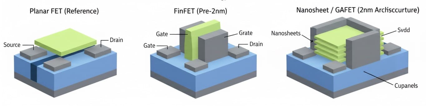
Evolution from Planar to FinFET to Nanosheet.
At 2nm, FinFETs hit a physical wall where current bleeds through the channel even when turned off. Gate-All-Around (GAA) nanosheet technology solves this by suspending individual, ultra-thin horizontal sheets of silicon completely surrounded by the gate material on all four sides. Enclosing the channel entirely provides maximum electrostatic control, drastically reduces parasitic current leakage, and allows chip designers to tune nanosheet widths for optimal performance or power efficiency.
Analysis
In 30 years covering tech markets, semiconductor performance gains were historically driven by geometric scaling—simply shrinking feature sizes made chips faster, cheaper, and more energy-efficient. That classical scaling model hit severe physical limits below 5nm.
To understand how drastically line widths have contracted over the last half-century, the table below maps the decline in process nodes by decade:
| Decade | Leading-Edge Line Width Range | Key Structural Paradigm |
|---|---|---|
| 1970s | 10,000 nm (10 µm) – 3,000 nm (3 µm) | Planar silicon MOSFETs |
| 1980s | 2,000 nm (2 µm) – 800 nm (0.8 µm) | Sub-micron planar CMOS |
| 1990s | 600 nm (0.6 µm) – 180 nm (0.18 µm) | Deep sub-micron optical lithography |
| 2000s | 130 nm – 32 nm | High-k metal gate (HKMG) planar transition |
| 2010s | 22 nm – 7 nm | 3D FinFET architecture |
| 2020s | 5 nm – 2 nm | Gate-All-Around (GAA) Nanosheets |
| 2030s (Est.) | Sub-1 nm / Angstrom Era (A14 – A2) | Complementary FET (CFET) & 2D Monolayer Materials |
Beyond 1nm: The Next Architectural Dimensions
The semiconductor industry will reach the sub-1nm threshold through fractional steps rather than a single jump. At atomic scale, quantum tunneling prevents standard horizontal scaling. Manufacturers are pivoting to new physical dimensions:
- Vertical Spatial Scaling (CFET & 3D Chiplets): Complementary FET (CFET) stacks n-channel and p-channel transistors on top of each other, cutting footprint in half. Higher up, 3D chiplet stacking places memory and logic directly above one another to shorten interconnect distances.
- Backside Power Delivery Networks (BSPDN): Traditional chips route both power lines and data signals on the front surface, causing resistance and interference. Moving power delivery to the back of the silicon wafer frees up signal layers and cuts voltage drops.
- 2D Monolayer Channel Materials: Replacing bulk silicon with single-atom-thick semiconductor materials, such as molybdenum disulfide (MoS2), maintains electron mobility in channels only a few angstroms thick.
- Architectural Specialization: General-purpose compute scaling is shifting toward heterogeneous packaging (such as TSMC’s CoWoS), domain-specific custom accelerators, and optical interconnects.
Enterprise Guidance
Enterprise infrastructure leaders should treat AMD’s 2nm announcement as a critical trend to understand deeply today and evaluate for deployment during upcoming hardware lifecycle refreshes.
- Audit Power Density Capacities: Organizations facing strict data center power limits should evaluate 2nm server hardware during 2026 and 2027 refresh cycles to increase compute density per watt
- Focus on Architecture Over Clock Speed: Evaluate platform architecture, memory bandwidth integration, and interconnect speeds rather than raw megahertz.
- Model Total Cost of Ownership: Wafer costs for GAA nodes carry premium pricing. Compute return on investment using energy savings and server consolidation ratios rather than unit silicon costs.
Impact on the Market
The arrival of production-grade 2nm manufacturing accelerates market concentration across the semiconductor supply chain. Capital expenditure required for sub-2nm fabrication centers limits advanced foundry capabilities to a tiny group of manufacturers, maintaining strong market dependence on TSMC.
In addition, processor vendors that master heterogeneous chiplet design and 3D packaging will widen their advantage over vendors relying purely on monolithic silicon shrinks. In the enterprise server segment, this dynamic will intensify competition between x86 platforms and custom ARM silicon developed by hyperscalers, compelling traditional chip makers to deliver tighter hardware-software optimization.
Bottom Line
AMD’s 2nm announcement confirms that Gate-All-Around nanosheets are commercially viable, but it also signals the end of traditional two-dimensional silicon scaling. As the industry approaches sub-1nm limits, performance gains over the next decade will rely on 3D spatial integration, backside power networks, and advanced packaging. Enterprise CIOs should evaluate 2nm systems for high-density AI and enterprise workloads while preparing for a multi-dimensional, chiplet-driven future.
Related Blogs:
Google Teases Gemini 4 after Record Q2
How Anthropic won the PR Narrative but Google kept the Volume
Google Nano Banana: Free AI Image Tools for All
Dialpad & Google: Deep AI Integration
Important Research related to this Blog:
Also – Check out all our Podcasts HERE
Have a Comment on this?